The Rise of the AI-Defined Fab: How Accelerated Computing and Physics-Based Intelligence are Reshaping Semiconductor Manufacturing

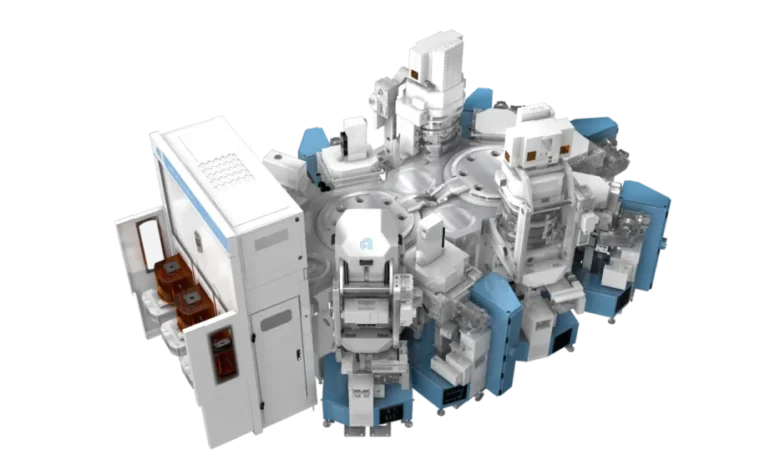
Global demand for increasingly advanced, highly sophisticated microchips has reached unprecedented heights, driven by rapid expansions in artificial intelligence, cloud computing, and next-generation consumer electronics. However, this surging demand collides directly with fundamental physical limits. As semiconductor manufacturing processes grow exponentially more complex, the margin for operational error has shrunk to nearly atomic scales. For modern semiconductor engineers, determining how a minute process change will behave, evaluating how novel materials interact during an unfamiliar fabrication step, or tracing a microscopic defect back to its primary root cause have historically been exceptionally challenging undertakings. These critical analyses routinely consumed days or even weeks of painstaking manual work.
Physical experimentation on an active fabrication line, or fab, is inherently slow, capital-intensive, and fraught with risk. In the high-stakes economics of semiconductor fabrication, making an incorrect decision regarding yield optimization, material selection, or overall process quality carries multi-million-dollar consequences. To overcome these bottlenecks, the semiconductor industry is undergoing a profound structural transformation. By integrating accelerated computing, physics-based artificial intelligence, autonomous workflow agents, and photorealistic digital twins, manufacturers are pioneering a new paradigm: the AI-defined fab. This technological evolution does not replace human expertise; rather, it empowers engineers to optimize workflows, preemptively catch catastrophic defects, and make highly informed decisions across the entire semiconductor manufacturing lifecycle with unprecedented speed.
The Evolution of Semiconductor Complexity and the Computational Bottleneck
To understand the necessity of an AI-defined fab, one must examine the historical trajectory of semiconductor scaling. For decades, the industry relied primarily on geometric scaling—shrinking transistors to fit more computing power onto a single piece of silicon. As nodes crossed into the sub-nanometer threshold, traditional manufacturing techniques encountered severe physical barriers, including quantum tunneling effects, extreme thermal dissipation, and severe lithographic diffraction limits.
By the early 2020s, traditional central processing units (CPUs) running sequential workloads could no longer keep pace with the massive computational requirements of modern design verification and process simulation. Simulating the complex interactions of light, plasma, and atomic-scale deposition required running millions of heavy differential equations. Consequently, research and development cycles lengthened, and the cost of building new fabrication plants skyrocketed past the twenty-billion-dollar mark.
Recognizing these systemic challenges, technology leaders began exploring heterogeneous computing architectures. Over the past five years, the convergence of parallel processing hardware and specialized software libraries has catalyzed a shift from purely physical trial-and-error manufacturing to predictive, software-driven simulation. Industry collaborations between computing pioneers like NVIDIA and manufacturing giants such as Applied Materials, Siemens, Lam Research, and COMSOL have systematically replaced legacy computational frameworks with accelerated platforms capable of compressing weeks of multi-physics simulation into mere minutes.
Accelerated Computing Radically Expands Engineering Exploration
The integration of accelerated computing into semiconductor workflows changes more than just the speed of individual calculations; it fundamentally alters the breadth of exploration available to design and process engineers. In traditional environments, computational limitations forced teams to test a severely restricted subset of potential process variations, increasing the risk of unforeseen failures during physical production runs.
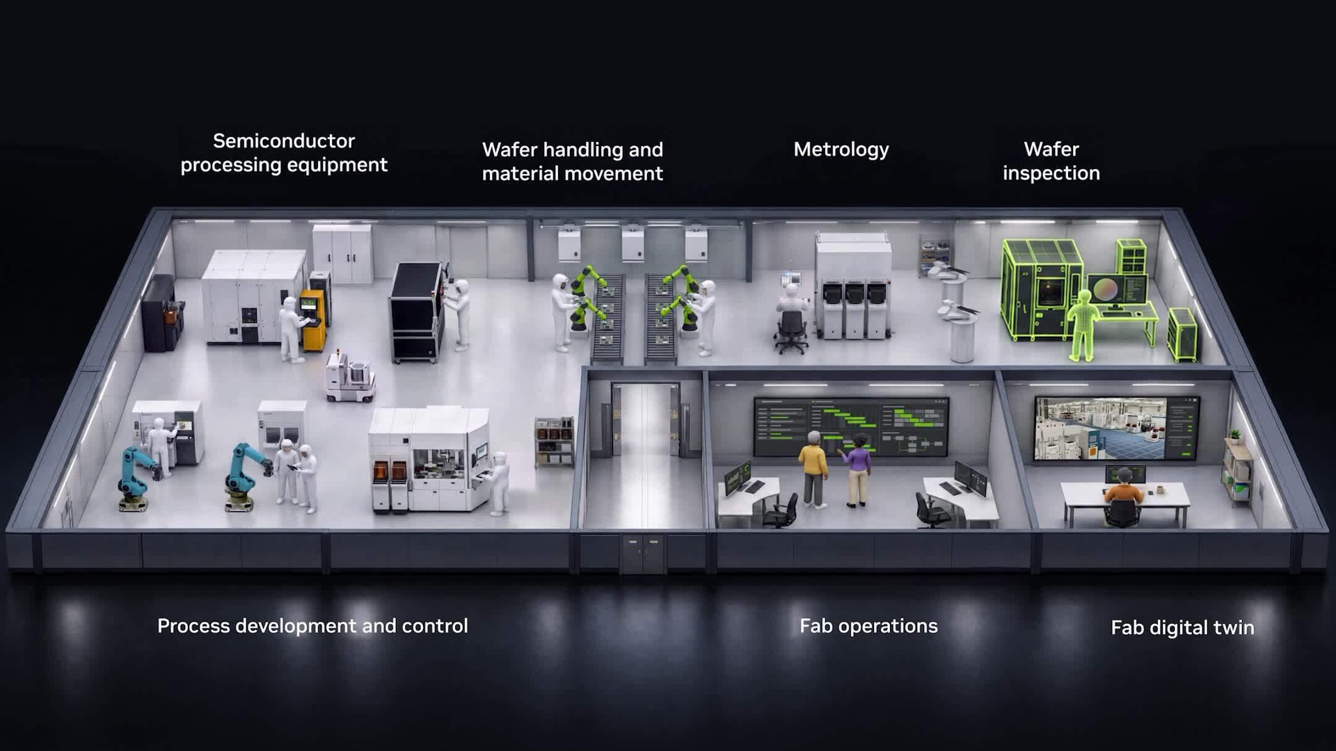
Multiphysics simulations—which model the simultaneous interactions of complex physical phenomena, such as thermal transfer, electrical current distribution, and mechanical stress—are essential for designing robust manufacturing equipment. Through the adoption of specialized libraries like NVIDIA cuDSS, software providers have unlocked massive performance gains. For instance, COMSOL has accelerated its multiphysics simulations for semiconductor manufacturing by up to tenfold, allowing engineers to rapidly optimize equipment configurations and evaluate multiple process alternatives before committing to expensive physical trials.
Similarly, Applied Materials has collaborated extensively with NVIDIA to revolutionize atomic-scale materials discovery and process development. By integrating the cuDSS library into its Ginestra simulation platform, Applied Materials achieved up to a tenfold speedup compared to conventional CPU-only architectures. Furthermore, the incorporation of NVIDIA PhysicsNeMo into Applied Materials’ ACE+ multiphysics platform has enabled topography simulations to run up to 35 times faster.
In critical areas like computational lithography—the mathematical processing required to print intricate circuit patterns onto silicon wafers—computational intensity has historically restricted full-scale verification. Siemens has directly integrated NVIDIA cuLitho into its industry-standard Calibre lithography software, yielding up to a 17-fold acceleration on key simulation workloads. This technological leap allows engineers to verify vastly larger portions of a chip layout before a single physical wafer goes to print, dramatically reducing the probability of costly manufacturing re-spins.
Predicting Process Behavior via Physics-Informed Artificial Intelligence
While accelerated computing drastically reduces the time required for traditional numerical solvers, certain semiconductor manufacturing phenomena remain computationally prohibitive even on high-performance hardware. To address this, the industry has turned toward physics-informed artificial intelligence, where machine learning models trained on fundamental physical laws can predict process behavior without executing full-scale simulations every time.
The impact of this approach is most evident in the modeling of plasma, an electrically charged gas utilized extensively in advanced semiconductor etch processes. Accurately modeling plasma behavior requires solving complex systems of equations that account for simultaneous electrical, chemical, and thermal interactions. Historically, these simulations required days of supercomputer processing time. By leveraging NVIDIA PhysicsNeMo, engineers can now generate highly accurate plasma-prediction simulations in mere milliseconds.
Building upon these advancements, Lam Research announced plans to integrate NanoVDB technology into its advanced semiconductor process modeling platform, SEMulator3D, a key offering within the company’s Semiverse Solutions portfolio. This integration is projected to accelerate select wafer-etch modeling processes by up to 30 times, enabling unprecedented predictive insight into how microscopic trenches and features are etched into silicon wafers during advanced 3D NAND and gate-all-around (GAA) transistor fabrication.
Autonomous AI Agents Streamline Complex Engineering Workflows
Beyond simulation and prediction, semiconductor manufacturing involves vast quantities of sequential, administrative, and analytical tasks that consume valuable engineering hours on the test and fabrication floor. The evaluation and selection of appropriate AI models for specific diagnostic or optimization tasks, for example, has traditionally been a manual, time-consuming process.
To eliminate these routine bottlenecks, companies are deploying autonomous AI agents capable of orchestrating complex sequences of engineering tasks. Advantest, a leading provider of semiconductor test equipment, has implemented NVIDIA NeMo Switchyard AI agents to automate model selection and workflow routing. This intelligent automation has successfully reduced system response times from hours down to minutes, allowing test floor engineers to focus their expertise on high-level problem-solving and yield enhancement rather than routine software configuration.
Virtualizing the Factory Floor with Photorealistic Digital Twins
As semiconductor fabrication facilities grow increasingly complex, the financial and operational risks of altering factory layouts, material logistics, or equipment configurations have multiplied. To mitigate these risks, modern manufacturers are turning to digital twins—hyper-realistic virtual replicas of physical fabs that simulate every facet of factory operations before changes are deployed on the physical line.
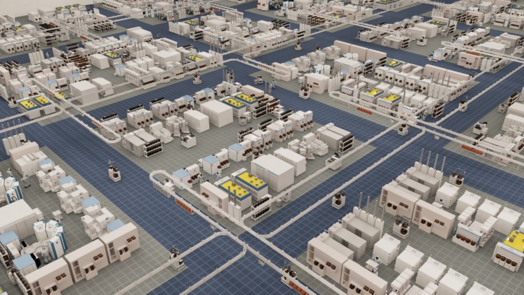
Applied Materials has leveraged NVIDIA Omniverse libraries to construct physically accurate, photorealistic digital twins of entire semiconductor fabrication plants. These virtual environments allow operational teams to simulate complex material movement, identify micro-bottlenecks in transport systems, and evaluate factory-wide layouts and operating strategies. By extending virtual experimentation beyond individual process chambers to encompass the entire factory floor, manufacturers can optimize throughput, lower operational costs, and validate risk mitigation strategies in a completely safe virtual domain.
The Connected Loop and Future Industry Implications
The ultimate realization of the AI-defined fab lies in the establishment of a continuous, closed-loop ecosystem. In this integrated workflow, real-time production data gathered from the fabrication line continuously feeds and refines predictive AI models. These models evaluate potential process modifications, and the resulting insights are delivered directly to engineers, who make informed, high-level production decisions.
Industry analysts project that the widespread adoption of AI-defined manufacturing principles will substantially shorten time-to-market for next-generation microchips, improve overall manufacturing yields, and partially offset the staggering capital expenditures required to build modern semiconductor foundries. As global competition intensifies and process nodes approach atomic dimensions, the ability to learn from every production cycle and act upon those insights with software-defined speed will define the market leaders of the 21st-century semiconductor industry.